General Description
The Evaluation Board demonstrates the RT9147 to be designed for a 20V/1A low power, high slew rate, single supply rail-to-rail input and output operational amplifier. The RT9147 ontains two amplifiers in one package. The RT9147 has a high slew rate (35V/μs), 1A peak output current and offset voltage below 15mV. The RT9147 is ideal for Thin Film Transistor Liquid Crystal Displays (TFT-LCD).
Performance Specification Summary
Summary of the RT9147ZQW Evaluation Board performance specificiaiton is provided in Table 1. The ambient temperature is 25°C.
Table 1. RT9147ZQW Evaluation Board Performance Specification Summary
|
Specification
|
Test Conditions
|
Min
|
Typ
|
Max
|
Unit
|
|
Supply Range
|
|
6
|
--
|
20
|
V
|
|
Peak Output Current
|
|
800
|
1000
|
1400
|
mA
|
|
Input offset Voltage
|
VCM = VS+ / 2
|
--
|
2
|
15
|
mV
|
|
Common Mode Rejection Ratio
|
0.5V < VOUTX <VS+ - 0.5V
|
--
|
95
|
--
|
dB
|
|
Power Supply Rejection Ratio
|
VS+ = 6V to 20V, VCM = VOUTx = VS+ / 2
|
--
|
96
|
--
|
dB
|
|
Slew Rate
|
4V step, 20% to 80%, AV = 1
|
--
|
35
|
--
|
V/µs
|
|
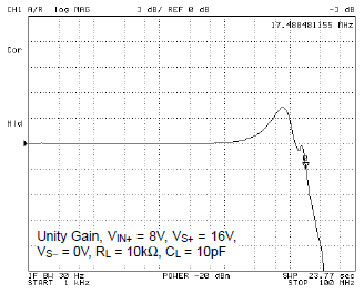
-3dB Bandwidth
|
RL = 10kΩ, CL = 10pF
|
--
|
16
|
--
|
MHz
|
|
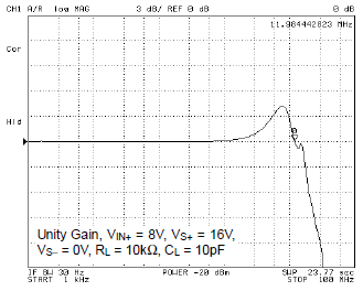
Gain-Bandwidth Product
|
RL = 10kΩ, CL = 10pF
|
--
|
12
|
--
|
MHz
|
|
Phase Margin
|
RL = 10kΩ, CL = 10pF
|
--
|
50°
|
--
|
--
|
Power-up Procedure
Suggestion Required Equipments
- RT9147ZQW Evaluation Board
- DC power supply capable of at least 20V and 1A
- Network Analyzer
- Function Generator
- Oscilloscope
Quick Start Procedures
The Evaluation Board is fully assembled and tested. Follow the steps below to verify board operation. The default connection is under configuration of unity gain buffer. Do not turn on supplies until all connections are made. When measuring the output voltage ripple, care must be taken to avoid a long ground lead on the oscilloscope probe. Measure the output voltage ripple by touching the probe tip and ground ring directly across the last output capacitor.
Proper measurement equipment setup and follow the procedure below.
1) With power off, connect the input power supply to VS+ and VS- pins.
2) With power off, connect the oscilloscope between the VOUT and nearest GND pins.
3) Turn on the power supply at the input. Make sure that the input voltage does not exceeds 20V on the Evaluation Board.
4) Check for the proper output voltage using a voltmeter.
5) Once the proper output voltage is established, adjust the load within the operating ranges and observe the output voltage regulation, ripple voltage, efficiency and other performance.
Detailed Description of Hardware
Headers Description and Placement
Carefully inspect all the components used in the EVB according to the following Bill of Materials table, and then make sure all the components are undamaged and correctly installed. If there is any missing or damaged component, which may occur during transportation, please contact our distributors or e-mail us at evb_service@richtek.com.
Test Points
The EVB is provided with the test points and pin names listed in the table below.
|
Test Point/
Pin Name
|
Function
|
|
VS+
|
Positive supply input.
|
|
VS-
|
Negative supply input.
|
|
GND
|
Ground.
|
|
VOUTA
|
Output of Amplifier A.
|
|
VINA−
|
Negative input of Amplifier A.
|
|
VINA+
|
Positive input of Amplifier A.
|
|
VOUTB
|
Output of Amplifier B.
|
|
VINB−
|
Negative input of Amplifier B.
|
|
VINB+
|
Positive input of Amplifier B.
|
|
VP
|
Positive voltage source for resister divider to VINA+ and VINB+.
|
|
VN
|
Positive voltage source for resister divider to VINA- and VINB-.
|
Bill of Materials
|
Unity Gain Buffer Configuration
|
|
Reference
|
Count
|
Part Number
|
Value
|
Description
|
Package
|
Manufacturer
|
|
U1
|
1
|
RT9147ZQW
|
RT9147ZQW
|
Rail-to-Rail OPa
|
WQFN-16L 4x4
|
RICHTEK
|
|
CIA1, CIB1
|
2
|
0805B104K500
|
0.1µF
|
Capacitor, Ceramic, 50V/X7R
|
0805
|
WALSIN
|
|
CS+
|
1
|
0603X105K250CT
|
1µF
|
Capacitor, Ceramic, 25V/X5R
|
0603
|
WALSIN
|
|
CS-, RIA1
|
2
|
WR06X000 PTL
|
0
|
Resistor, Chip, 1/10W, 5%
|
0603
|
WALSIN
|
|
RIAN2, RIB1, RIBN2
|
3
|
RTT05000JTP
|
0
|
Resistor, Chip, 0.125W, 5%
|
0805
|
RALEC
|
Typical Applications
EVB Schematic Diagram
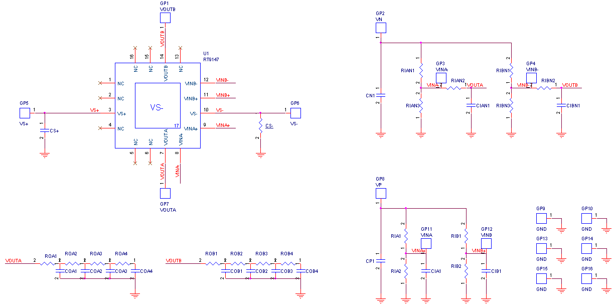
1. The capacitance values of the input and output capacitors will influence the input and output voltage ripple.
2. MLCC capacitors have degrading capacitance at DC bias voltage, and especially smaller size MLCC capacitors will have much lower capacitance.
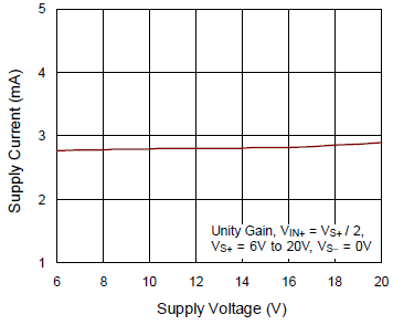
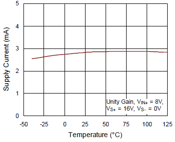
Measure Result
|
Supply Current vs. Supply Voltage
|
Supply Current vs. Temperature
|
|
|
|
|
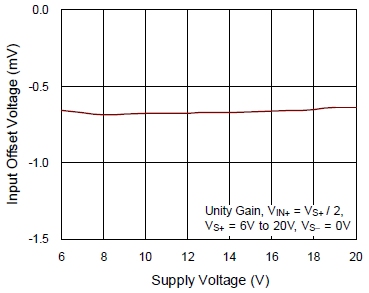
Input Offset Voltage vs. Supply Voltage
|
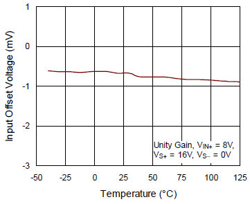
Input Offset Voltage vs. Temperature
|
|
|
|
|
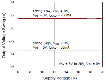
Output Voltage Swing vs. Supply Voltage
|
Rail to Rail
|
|
|
|
|
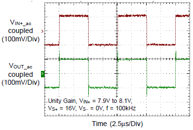
Small Signal Response
|
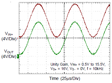
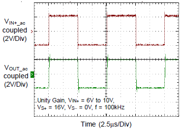
Large Signal Response
|
|
|
|
|
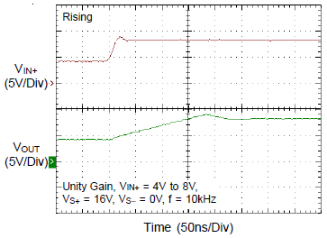
Slew Rate
|
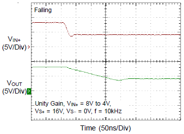
Slew Rate
|
|
|
|
|
−3dB Bandwidth
|
Gain Bandwidth Product
|
|
|
|
Note: When measuring the input or output voltage ripple, care must be taken to avoid a long ground lead on the oscilloscope probe. Measure the output voltage ripple by touching the probe tip directly across the output capacitor.
Evaluation Board Layout
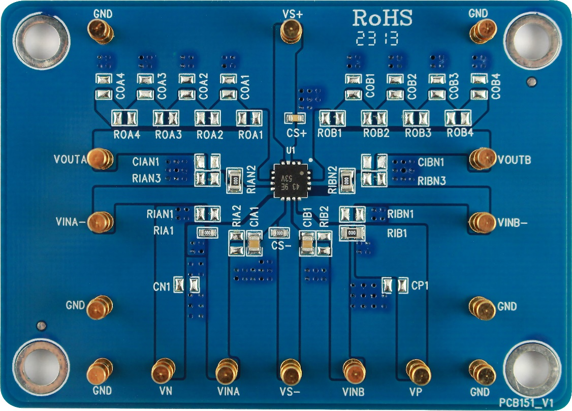
Figure 1 to Figure 2 are RT9147ZQW Evaluation Board layout. This board size is 70mm x 50mm and is constructed on four-layer PCB, outer layers with 2 oz. Cu and inner layers with 1 oz. Cu.
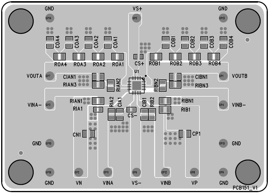
Figure 1. Top View (1st layer)
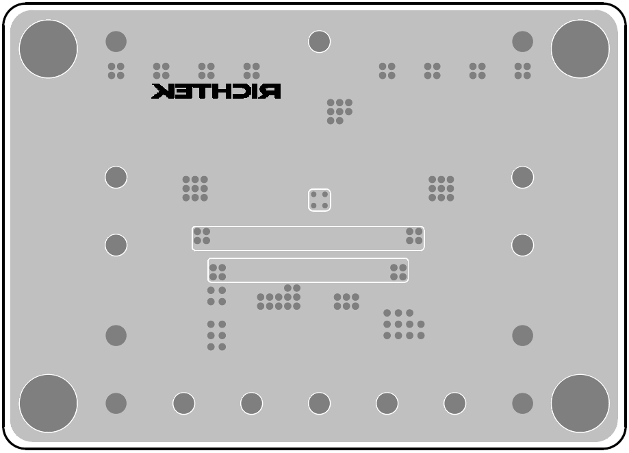
Figure 2. PCB Layout—Bottom View (2nd Layer)